The construction on printed circuit boards is largely final.
Therefore a circuit should be
- be tested on a plug-in board.
- Also, before starting the layout.
Modern circuits are mostly built on printed circuit boards. These are about 1.5mm thick sheets of plastic:
- Pertinax – paper bound with plastic,
- GRP – glass fiber reinforced plastic – mostly epoxy resin.
On the surface of the printed circuit board are "printed" connections of copper foil, conductive traces. In the printed circuit board there are holes for mounting components.
The components are soldered to the traces, either with wires that are put through holes, through hole technology (THT) or directly onto the trace, SMD technology.
The production of printed circuit boards includes
- the design of the traces and the position of the components, the creation of the layout,
- the application or. Creating the traces,
- Cutting the printed circuit board,
- the drilling of the printed circuit board and
- The soldering of the components.
Sides of the printed circuit board
In the conventional technology the components are mounted on one side of the circuit board. This side is therefore often referred to as the component or assembly side. Connectors are inserted through holes in the PCB and soldered on the other side of the PCB (solder side). On the solder side there are conductive tracks. Printed circuit boards that only have traces on the solder side are called single-sided printed circuit boards. On the assembly side, connections are sometimes made with wire jumpers.
Modern printed circuit boards also have conductive tracks on the assembly side. The printed circuit board has two layers. More complex circuits can have multiple interlayers: Multi-layer Technology.
The connections between the layers are made by plated through holes. Holes that only serve to connect between layers are called vias.
Modern technology uses surface mount devices, SMD. The connections are no longer inserted through drilled holes, but soldered directly onto the surface. The components can be mounted on both sides of the PCB.
In this sense we cannot speak of component and solder side. We better use top and bottom side.
Examples of printed circuit boards
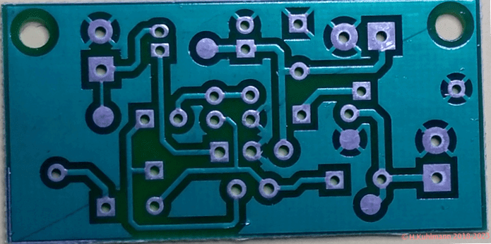
Figure 1 shows a PCB with the printed traces and the holes for components. The printed circuit board is made of GRP epoxy.
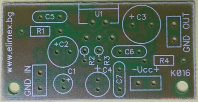
The printed circuit board in Figure 2 has an imprint on the top side for placement purposes.
The printed circuit board in Fig. 1 and Fig. 2 has tracks on one side only. Only through-hole technology is used.
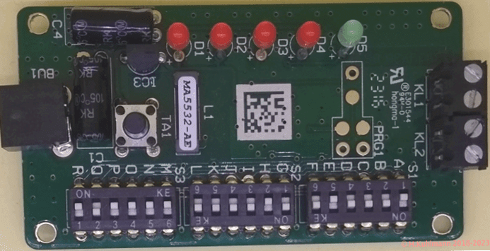
The top side of the PCB in picture 3 with a complex circuit is almost exclusively equipped with wired components. It is also provided with conductive tracks on the upper side. The PCB is made of GRP epoxy.
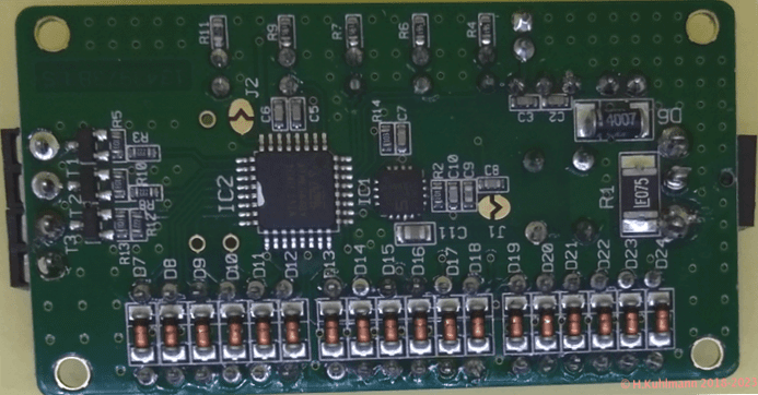
The printed circuit board in pictures 3 and 4 is populated on the bottom side with SMD components only. This circuit board uses a mixture of SMD and through-hole technology.
The printed circuit board was prefabricated. The SMD components were already assembled. Only the components with connections for the through-hole technology still had to be installed.
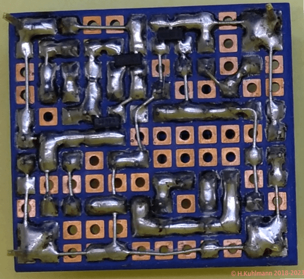
On the underside of the printed circuit board with hole pattern in Fig. 5, the connections are made with thin wires. In addition, three simple SMD components are soldered on. The printed circuit board is made of GRP epoxy.
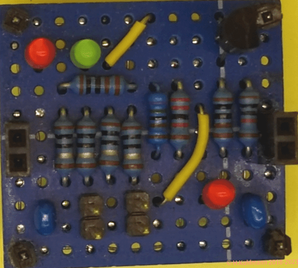
On the top side of the PCB in pictures 5 and 6 there are only components in through-hole technology. Two connections were made with yellow wire jumpers.
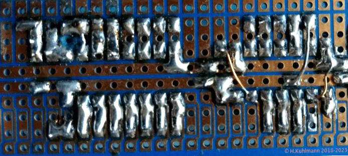
Strip grids are well suited for digital components in DIL packages. The strip grid in Fig. 7 has two long strips between the DIL rows, which are used for the power supply.